Workflow
- Capture the AFM scan: run the surface scan on the Park Systems NX10, ensuring good tip engagement and appropriate scan parameters for the feature scale
- Export height data: export the raw height matrix from NanoScope/Park software
- Convert to STL: process the height data through an online height-map-to-STL converter
- Mesh cleanup: open STL in slicer, verify the mesh is manifold and printable; adjust scale so features are at a printable size
- Print: FDM print with fine layer height settings; inspect against the original scan
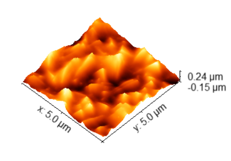
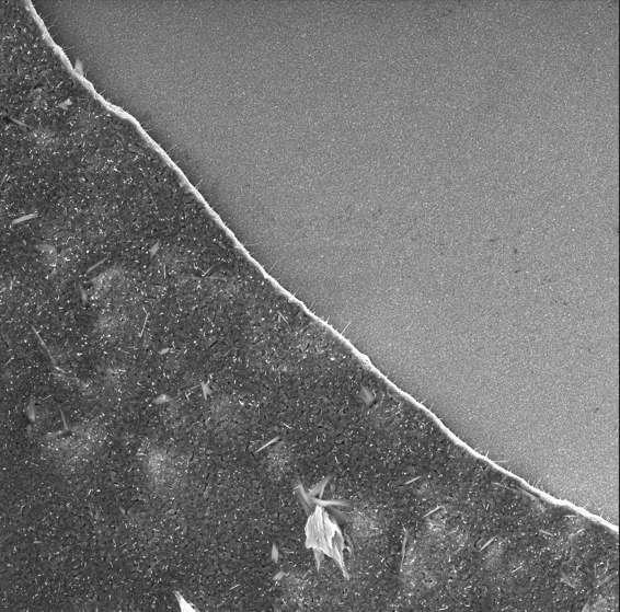
AFM scan showing raw height data
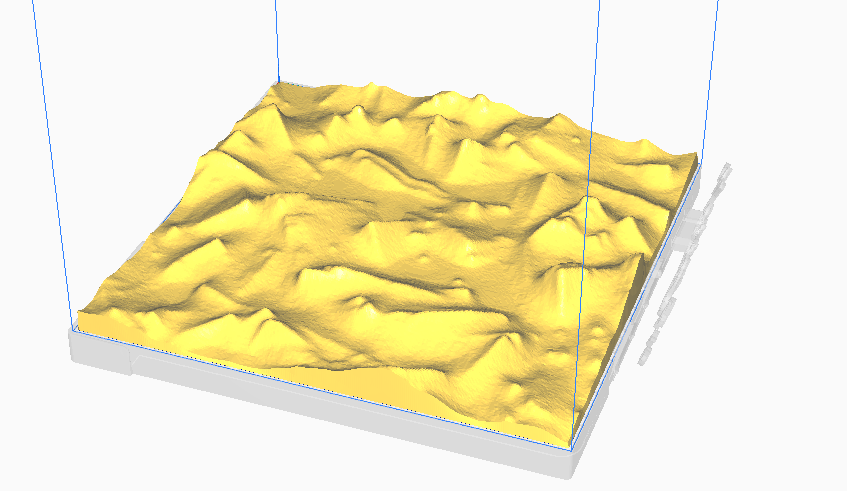
STL file preview in slicer
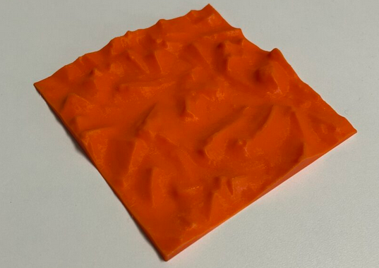
3D printed physical model
The Challenge: Noise and Artifacts
AFM data always contains artifacts: tip convolution, scanner drift, line noise. Some can be flattened in post-processing. The challenge is distinguishing real surface features from measurement artifacts before sending the file to the printer.
Most scans are unsuitable for printing because their structures either don't translate to a printable feature size, or the noise level makes the mesh unprintable. The best candidates are surfaces with well-defined features at a scale that maps cleanly to a printable geometry, such as periodic structures, clearly resolved particles, or step edges.
Filtering Criteria for Printable Scans
- Feature height > ~5% of scan width (otherwise flattened to noise in print)
- Lateral feature size > ~0.5 mm at intended print scale
- Surface must not require support structures that would obscure features
- Noise floor low enough to produce a clean mesh without heavy smoothing
Current Status & Future Work
Still actively looking for samples with the right combination of feature size, periodicity, and low noise. The silicon thermal oxidation and CuO electrodeposition scans produced interesting surfaces but too much noise for clean printing.
Next steps:
- Test periodic structures (e.g., diffraction gratings, lithography test patterns) that have well-defined geometry
- Experiment with resin printing for higher resolution models
- Build a small set of successful physical surface models for lab outreach events
The AFM surface viewer renders real scan data as an interactive 3D heightmap in the browser.
Open AFM Surface Viewer