Process
Electrodeposition of Copper Oxide
- Cleaned substrate in ultrasonic bath with IPA and DI water
- Prepared 0.25M CuSO₄ solution; adjusted pH to 10 with NaOH and 3M lactic acid at ~50°C
- Masked substrate edges with Kapton tape to preserve FTO contact
- Deposited at -1.0V for 40 minutes with graphite counter electrode
- Rinsed with DI water and dried
Thermal Oxidation
- Removed Kapton; placed samples in box furnace at 425°C for 1 hour
- Cooled to below 20°C before opening
ZnO Sputtering
- Re-masked edges; used Zn target with pure O₂ as process gas
- Sputtered ~5 minutes
Aluminum Contact Deposition
- Kept masking; used Al target with Ar sputter gas; ~8 minutes
- Final thermal oxidation at 425°C for 1 hour
Fabricated solar cell on FTO glass substrate
Microscopy Results
AFM of CuO After Deposition
AFM after CuO deposition showed pronounced surface texturing. Some peaks appeared incomplete, likely due to inspecting the sample mid-deposition.
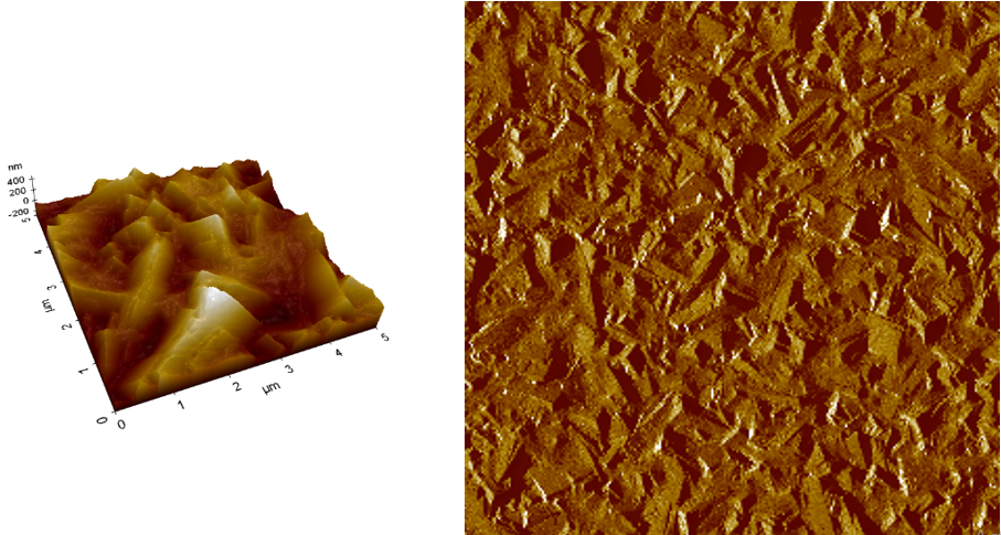
AFM scan of CuO surface after electrodeposition
SEM Results
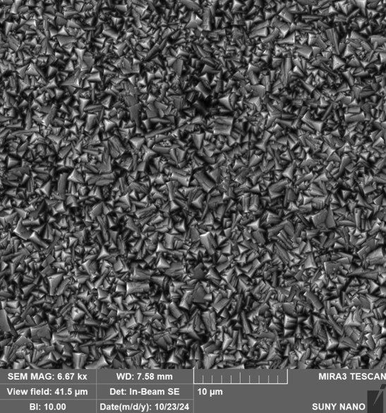
Copper Oxide pre-annealing: cubic/prismatic crystal morphology
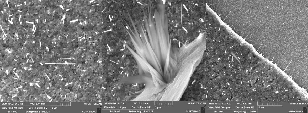
CuO post-anneal: porous surface with nanowire formation
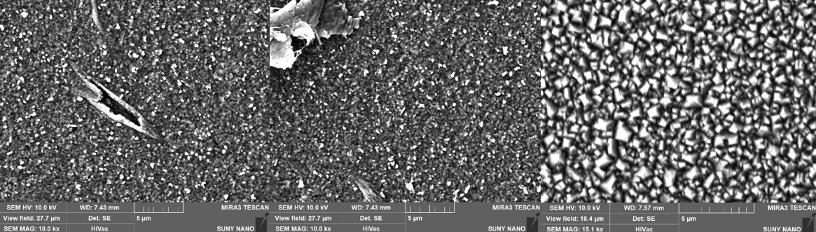
ZnO after sputtering
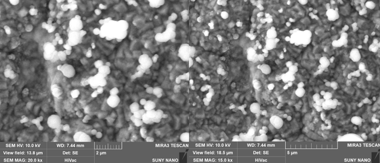
Aluminum contact layer
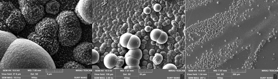
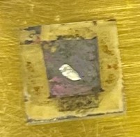
Failed attempt: loose contact during deposition caused non-uniform coverage and spherical particle formation
IV Characterization
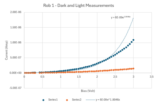
I-V curve under dark conditions
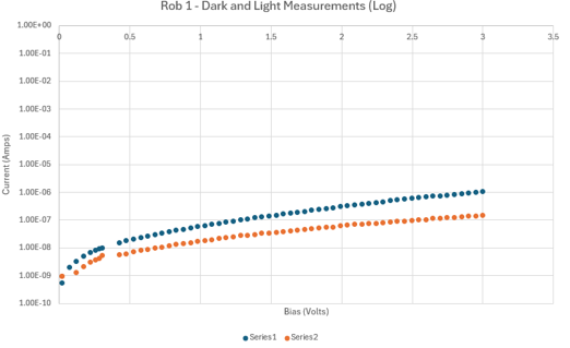
I-V curve under illumination
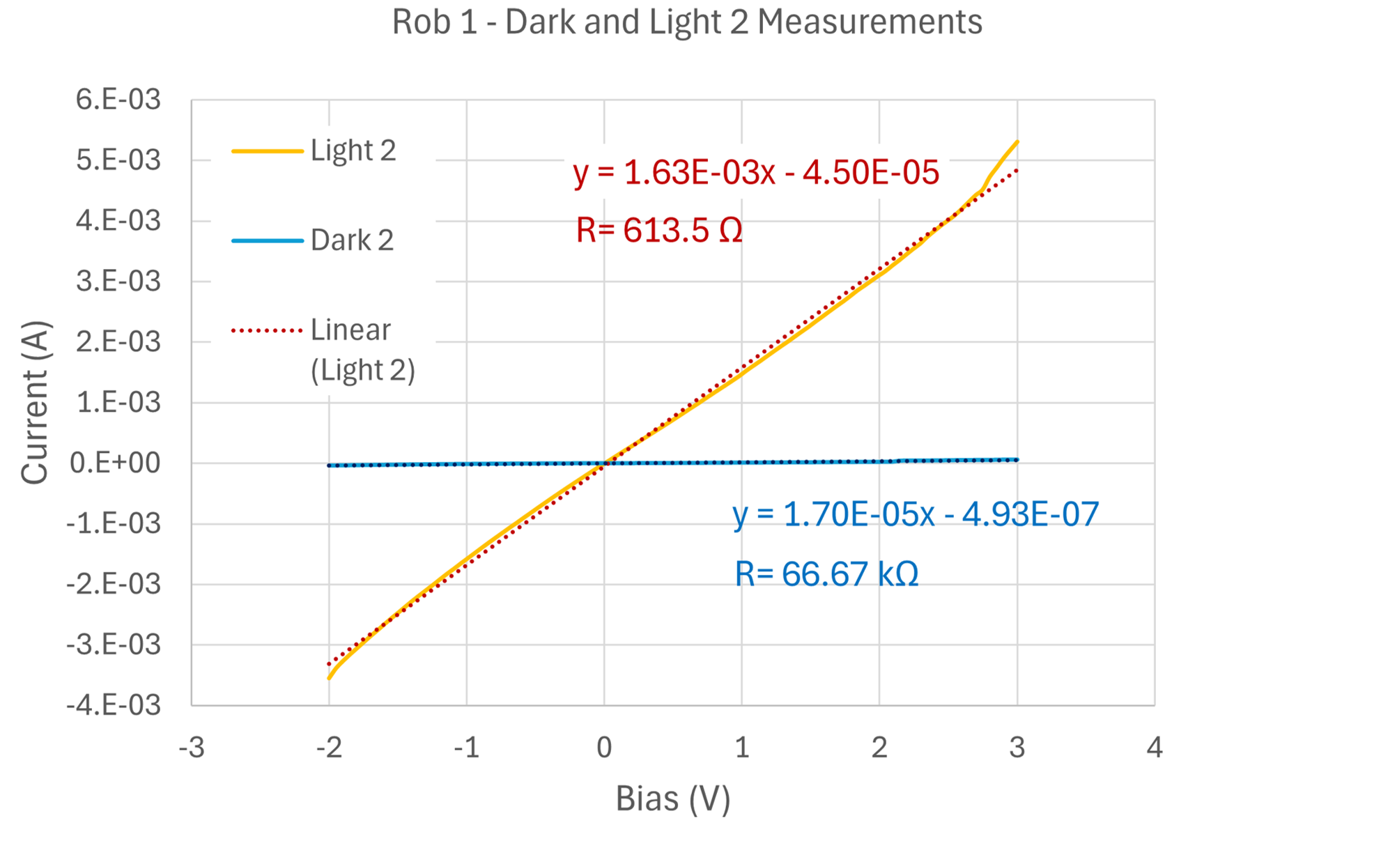
I-V curve comparison: dark vs. illuminated
Dark IV confirmed diode behavior. Under illumination, the curves suggested significant recombination losses consistent with the surface defects and non-uniform coverage visible in SEM. Shunt resistance was low, indicating leakage paths likely from the incomplete aluminum coverage and porous CuO layer.
Challenges & Lessons
- Handling samples between furnace steps introduced contamination; cleaning between each step (ultrasonic IPA + DI water) would reduce surface defects
- Loose contact during copper deposition on one sample caused non-uniform current density, visible as discontinuous regions and spherical particles in SEM
- Without introducing O₂ gas flow during oxidation, the growth rate diverged from simulation predictions
Future Work
- Tighter process control at each step, particularly cleaning between depositions
- Introduce proper dry O₂ flow during thermal oxidation steps
- Investigate conformal ZnO deposition to reduce interface defects
Thanks to Prof. Iulian Gherasoiu and Tyler Allen for guidance and lab support.