Simulation Setup
- Used NanoHub Process Lab: Oxidation tool to generate Deal-Grove growth datasets
- Parameters: Dry oxidation, 1200 min (20 hrs), initial thickness 30 nm, temperatures 900/1000/1100/1200°C, 2 atm pressure, Si(100)
- Extracted rate constants for Arrhenius analysis
Arrhenius Analysis
Plotted ln(rate constant) vs. 1/T (reciprocal absolute temperature).
- B/A (linear rate constant): surface reaction limited
- B (parabolic rate constant): diffusion limited
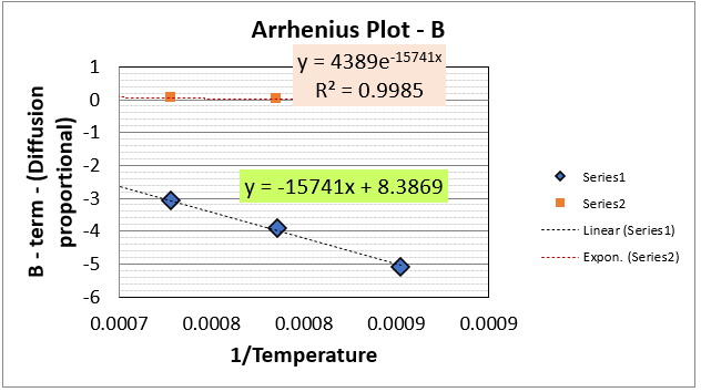
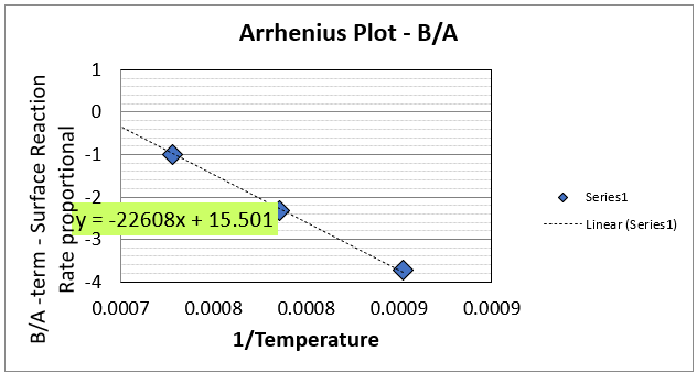
Activation energies were extracted by multiplying the negative slope by Boltzmann's constant. Extracted values compared favorably to literature, particularly for the diffusion-limited (B) regime.
Experimental Procedure
- Placed Si(100) wafer face-up in Thermo Scientific Lindberg Blue M box furnace
- Set 1000°C for ~20 hours
- Shut off and allowed several hours to cool; removed below 30°C
- Note: No O₂ or H₂O gas was introduced; growth relied on residual ambient oxidants
Equipment
| Equipment | Details |
|---|---|
| Silicon wafer | Polished, Si(001) |
| Furnace | Thermo Scientific Lindberg Blue M |
| SEM | Tescan Mira 3 |
| AFM | Park Systems NX10 |
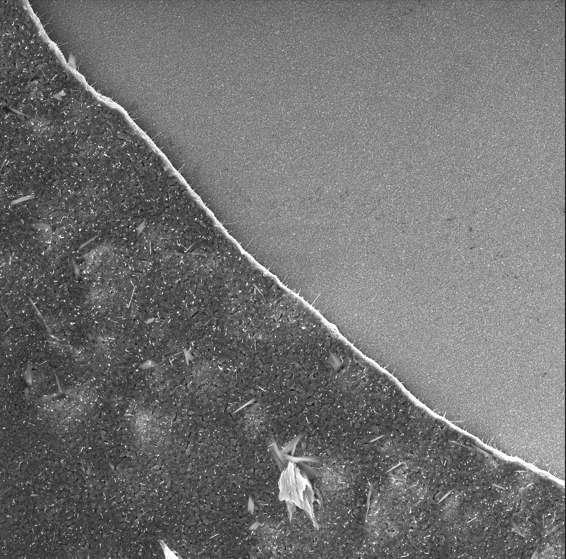
Visual Examination
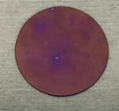
After oxidation, the wafer showed hues of carnation pink and red-violet under light. Using standard oxide color charts, these map to ~4200–6000 Å. The Deal-Grove simulation at 1000°C for 20 hours in dry O₂ predicted ~5600 Å. Because no O₂ was introduced during the actual run, growth was slower; the experimental thickness of ~4200 Å is consistent with ambient oxidation kinetics.
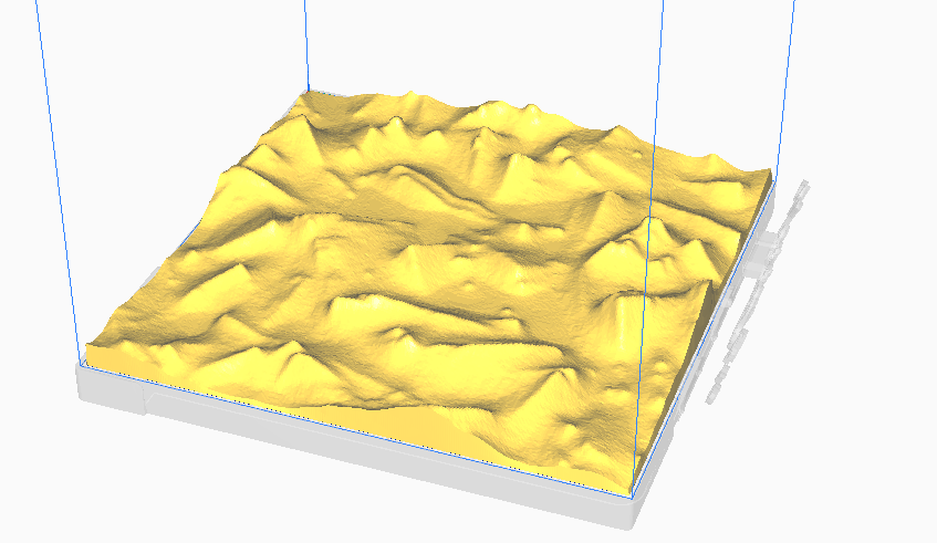
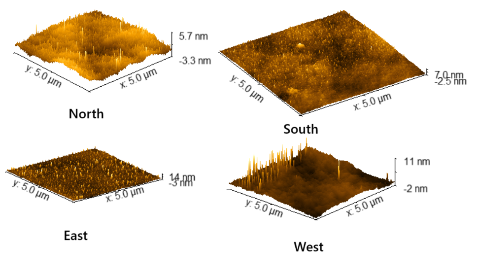
SEM and AFM Results

Conclusions & Future Work
The work demonstrated silicon oxidation behavior and provided hands-on experience linking Deal-Grove simulation to experiment. The sensitivity of the model to boundary conditions (gas flow, pressure, initial thickness) was clear from the divergence between simulated and experimental results.
Future iterations:
- Clean samples between steps (ultrasonic IPA + DI water) before imaging
- Follow defined dry/wet oxidation parameters with proper gas introduction
- Run multiple temperature points experimentally to build a real Arrhenius plot from measured data